The landscape of electronic device fabrication is undergoing a paradigm shift, thanks to groundbreaking advancements made by researchers at Rice University. Recently, a pioneering transfer-free technique for growing ultrathin semiconductors directly onto electronic components has emerged, promising to significantly enhance performance, reduce manufacturing complexity, and open doors to novel applications in flexible and wearable electronics.
Understanding the Traditional Challenges in Semiconductor Growth
Historically, the fabrication of ultrathin semiconductor layers has involved complex processes such as transfer engineering. In the conventional approach, semiconductors are grown on one substrate and then transferred onto another, involving numerous steps:
- Growth on ideal, crystalline substrates in controlled environments.
- Use of chemical or mechanical methods to detach the ultrathin layers.
- Transfer onto the target device substrates, which may introduce defects, strain, or contamination.
While effective, this transfer process is often laborious, costly, and can compromise the structural integrity of the ultrathin layers. These challenges have historically impeded the scalable adoption of ultrathin semiconductors in commercial electronics, especially in flexible or stretchable devices where durability and interface quality are critical.
The Breakthrough: Transfer-Free Growth Technique
Innovation Originating from Rice University
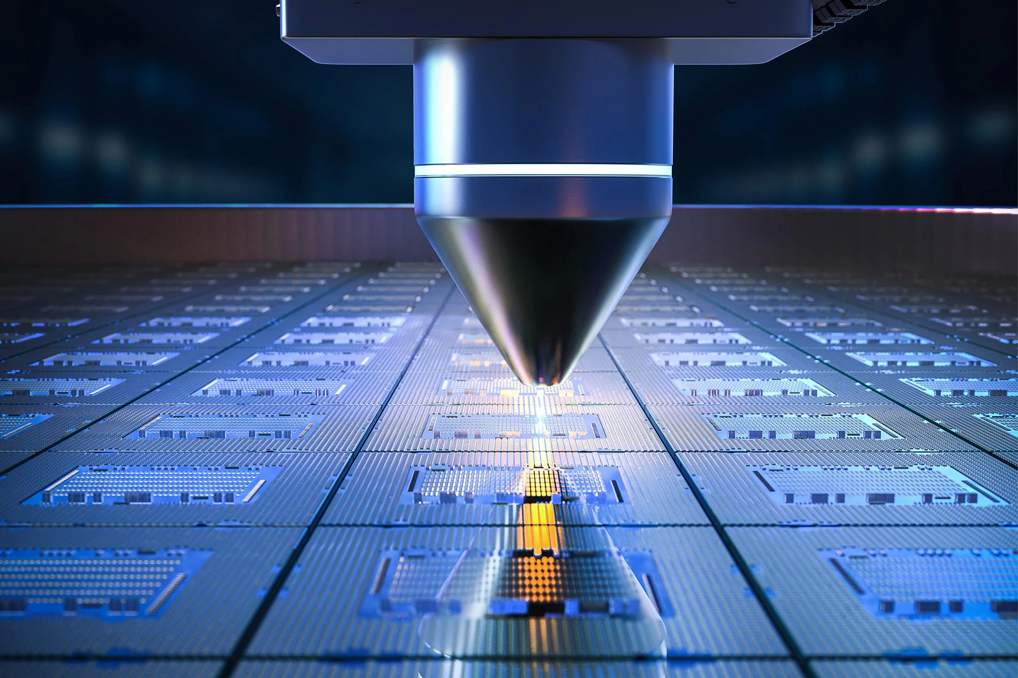
In a recent breakthrough, scientists from Rice University have developed a transfer-free method that allows for the direct growth of ultrathin semiconductors onto existing electronic substrates. This novel approach leverages advanced deposition techniques and substrate engineering to eliminate the need for post-growth transfer processes.
By growing the semiconductor in situ, researchers can produce high-quality, ultrathin layers that are strongly integrated with the device substrate, leading to a suite of advantages:
- Enhanced Interface Quality: Direct growth ensures atomically clean and defect-minimized interfaces.
- Reduced Production Steps: It simplifies manufacturing workflows, decreasing costs and time.
- Improved Mechanical Stability: The absence of transfer-related stress or strain enhances device durability.
- Compatibility with Flexible Electronics: The process is well-suited for flexible substrates, opening avenues for new form factors.
Technical Details & Methodology
The core of this technique involves sophisticated chemical vapor deposition (CVD) processes tailored for ultrathin film formation. The researchers employ methods such as:
- Optimized substrate preparation to promote nucleation and growth of the semiconductor directly on the target surface.
- Use of specific precursor gases and controlled temperature environments to facilitate layer-by-layer growth.
- Surface patterning and engineering to direct the growth and control the thickness at the atomic scale.
Through carefully controlled conditions, the team achieved the growth of monolayer and few-layer semiconductors like molybdenum disulfide (MoS₂) and tungsten diselenide (WSe₂) directly on various substrates, including flexible polymers and dielectric layers.
Implications for Future Technologies
What This Means for Electronics Industry
This technological advancement addresses several longstanding issues in the semiconductor industry:
- Scalability: The transfer-free method can be adapted for large-area production, crucial for commercial manufacturing.
- Device Performance: Ultrathin layers with pristine interfaces enhance electron mobility and reduce noise, leading to faster and more efficient devices.
- Miniaturization and Flexibility: The direct growth technique supports the development of ultra-compact, flexible, and wearable electronics, catalyzing innovations in biomedical devices, bendable displays, and IoT sensors.
- Environmental Benefits: Reducing process steps and chemical waste aligns with sustainable manufacturing goals.
Potential Applications
The transfer-free growth technique unlocks potential in multiple application domains, including:
- High-performance flexible transistors
- Next-generation wearable sensors
- Thin and transparent solar cells
- Miniaturized optoelectronic devices
- Advanced neuromorphic computing components
Challenges and Future Directions
While the transfer-free method offers numerous advantages, there remain challenges that the scientific community must address to facilitate widespread adoption:
- Uniformity and Reproducibility: Ensuring consistent quality over large areas remains a focus area.
- Material Compatibility: Extending the technique to a broader range of semiconductors and substrates.
- Integration into Existing Manufacturing Lines: Developing scalable and industry-compatible equipment is essential for commercial deployment.
Future research is directed toward refining growth parameters, exploring new materials, and integrating this method into existing semiconductor fabrication pipelines to create fully flexible, high-performance electronic systems.
Conclusion
The innovative transfer-free technique pioneered by Rice scientists represents a significant leap forward in the field of semiconductor fabrication. By simplifying the process, improving interface quality, and enabling direct growth on a variety of substrates—including flexible materials—this approach has the potential to revolutionize the design and manufacturing of ultrathin electronic devices. As research progresses and challenges are addressed, we can anticipate a new era of flexible, efficient, and miniaturized electronics that will underpin future technological innovations.
For more updated news please keep visiting Hourly Prime News.